
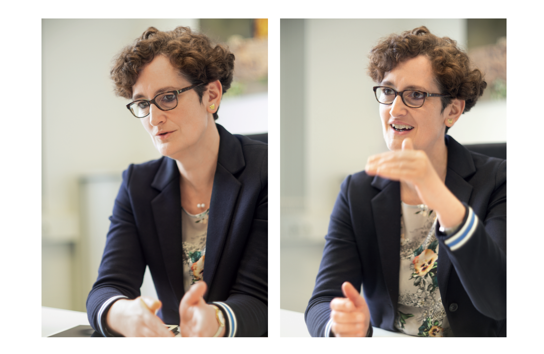
Katrin Ariki
Today, the majority of all microchips around the world is produced with technologies provided by the ZEISS Semiconductor Manufacturing Technology (SMT) segment. Last summer, ZEISS announced significant investments in its Wetzlar location. We spoke to the Site Director, Katrin Ariki.
W3+: I would ask if you like living in Wetzlar, but you’ve been here too long for that.
Katrin Ariki: Yes, I came to Wetzlar directly after studying in Göttingen and Innsbruck and worked here at a medium-sized optical company for three years. I joined ZEISS in 2001, signing my first job contract with Hensoldt AG, which already belonged to the ZEISS Group. The Semiconductor Manufacturing Technology segment already existed at that time, having been established in 1994. But I’d still like to answer your question: Yes, I feel quite at home here in Wetzlar. Otherwise, I surely wouldn’t have stayed for so long.
W3+: Presumably, a lot has changed in the SMT segment over the past 20 years.
Katrin Ariki: Absolutely. If you take a look at how the requirements of our final customers, the chip manufacturers, have developed with regard to the production of semiconductors and thus the quality and quantity demands placed on the ZEISS illumination systems, you will find huge differences between then and now. Back in 1968, ZEISS delivered the first lens for a circuitry printer. At that time, the forerunner to today’s wafer scanners for chip manufacturing was able to generate structures measuring about ten micrometers. These days, we’re much further along: Our latest lithography optics make it possible to generate structures measuring less than 20 nanometers.
W3+: Microchips have to be increasingly smaller, more powerful, faster and more energy-efficient. To what extent are you subjected to such technology or product cycles?
Katrin Ariki: For more than half a century, the semiconductor industry has managed again and again to produce a new chip generation every one or two years. Each generation has even more delicate structures and is even more powerful and efficient. The lithographic process carried out in the chip fabs is a key technology for achieving this. The lithography optics from ZEISS are the centerpiece of the machines created for exposing semiconductor wafers (wafer scanners) from our customer and partner, ASML.
Progressive digitalization requires new technologies, and this certainly also applies to Semiconductor Manufacturing Technology. Here, we consider ourselves enablers of technological leaps in entertainment, communication and vehicle electronics – consequently, we set the pace in digitalization to some degree. Look, for example, at how compact and powerful our mobile end devices are nowadays. This has a lot to do with the developments in semiconductor manufacturing. For instance, the latest generation of lithography optics with extreme ultraviolet light (EUV), which we developed together with our strategical partner ASML, make it possible to realize chip structures which are 4,000 times thinner than a human hair.
W3+: The ZEISS Group achieved record revenues in 2018 totaling approximately 5.8 million euros. In the first half-year of 2018/19, ZEISS reported further growth of nine percent. How does the ZEISS SMT segment contribute to this?
Katrin Ariki: The President & CEO of Carl Zeiss AG, Dr. Michael Kaschke, announced at the half-year press conference on 7 May that SMT achieved healthy growth despite the generally slow development in the semiconductor industry. In particular, this is due to the current generation of EUV lithography optics: the resulting revenue has increased significantly. This way, SMT was able contribute to the corporate success of the Group with five percent revenue growth in the first half of fiscal year 2018/19.
W3+: Regarding the market position of ZEISS: it sounds like high development costs are part the Semiconductor Manufacturing Technology’s business.
Katrin Ariki: Yes, that’s right. We invest a lot in the development of our systems. The ZEISS SMT segment has more than 3,800 employees, about 250 at the site in Wetzlar. About 30 percent of the employees work in research and development. Compared to other companies, this is a relatively high figure.
W3+: In summer 2018, ZEISS announced that the SMT segment would invest several million euros in its machinery at the Wetzlar location.
Katrin Ariki: SMT is headquartered in Oberkochen. But the site in Wetzlar is significant not only historically but also for the future. Wetzlar is one of the most important hubs for optics in Germany and around the globe. Over the decades, this is where the optical expertise we require for the production of state-of-the art lithography systems has evolved. You mentioned the investment in machinery – for this, we count on precision plants by Satisloh in Wetzlar and OptoTech Optikmaschinen in Wettenberg. As a result, we strengthen the regional economy, benefit from easy access to contacts within these companies, the prompt availability of spare parts and ongoing cooperation on improvement projects.
W3+: Speaking of optical expertise: Do you have any problems in finding qualified junior staff?
Katrin Ariki: We are in the fortunate position that ZEISS is an attractive brand, company and employer. What’s more, as a segment in the ZEISS Group, we can offer potential job candidates really excellent prospects throughout the company and even throughout the world. Thus, the question is really if their qualifications meet our requirements and what potential the candidates possess. In the highly specialized sector we operate in, we also see it as our task to train and help develop young employees ourselves. We train precision optics engineers and mechanics in-house for our production area. In Wetzlar, Jena and Oberkochen, we have vocational training workshops, which work closely with each other. In order to get skilled professionals for our robust engineering sector, we cooperate with the TH Mittelhessen University of Applied Sciences and support the new endowed professorship for Optics and Optical Technologies. In addition, we support several STEM programs to inspire high school students to take an interest in technical and science-oriented topics and professions.
W3+: Your commitment in and for the region can thus be seen as a commitment to the site?
Katrin Ariki: All too often, you get the impression that the decision for a location depends first and foremost on economic factors. Of course, a site has to contribute to the success of the whole enterprise, but we at ZEISS place great store in social responsibility. I’m very happy about that because, personally, I like doing something positive for the region where I live and work. This has been the case for more than 20 years. I feel quite at home here. But this was, in fact, basically the answer to your first question.
Company Profile:
ZEISS Semiconductor Manufacturing Technology (SMT) is one of four segments in the ZEISS Group. The segment generated revenues of more than € 1.5 billion worldwide in the fiscal year 2017/18. Optics for the Semiconductor Manufacturing Technology segment have been produced at the site in Wetzlar for more than 20 years. Lithography optics by ZEISS make it possible to produce chips which are ever smaller, more powerful, faster and more energy-efficient. These chips lay the foundation for microelectronic innovations like the internet of things, smart production as well as electromobility and autonomous driving.